Popular Searches:
Recommended Posts
Search Results
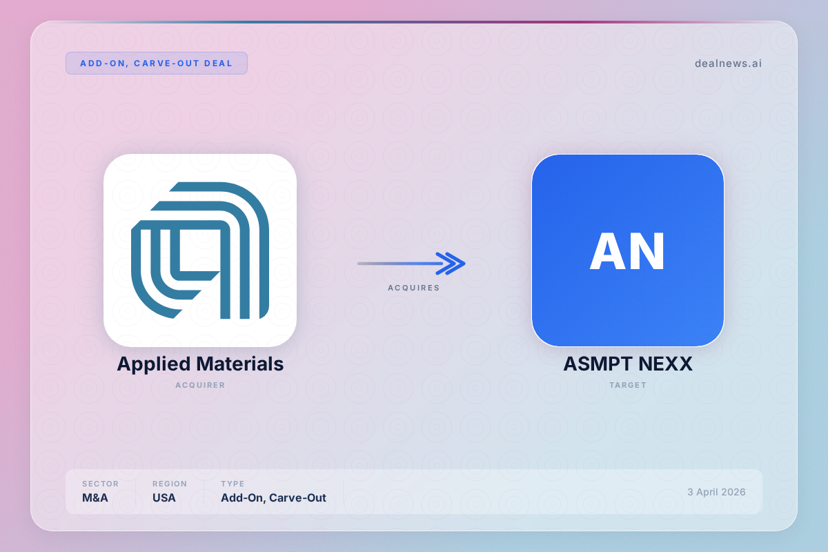
Applied Materials acquires NEXX business to expand advanced packaging tech for AI semiconductors. Learn about the strategic deal and market impact.
Applied Materials has entered into a definitive agreement to acquire the NEXX business from ASMPT Limited (HKEX: 0522), a leading supplier of large-area advanced packaging deposition equipment for the semiconductor industry. The acquisition, announced on May 3, 2026, aims to expand Applied’s portfolio of panel-level advanced packaging technologies, enabling chipmakers to develop larger, more energy-efficient AI accelerators.
The transaction, expected to close within several months subject to customary conditions, does not require regulatory approvals. Post-closing, the NEXX team will integrate into Applied’s operations and remain based in Billerica, Massachusetts.
While financial terms were not disclosed, the deal strategically adds NEXX’s panel-level electrochemical deposition (ECD) technology to Applied’s existing manufacturing systems, which include digital lithography, physical vapor deposition (PVD), chemical vapor deposition (CVD), etch, and eBeam metrology and inspection. This integration will support the growing demand for advanced packaging solutions that accommodate complex AI chip architectures such as 2.5D and 3D chiplet stacking.
Applied Materials, a Nasdaq-listed leader in semiconductor equipment and materials engineering, provides essential technology for semiconductor and advanced display manufacturing worldwide. The company focuses on advancing AI chip commercialization through innovative material solutions.
The NEXX business specializes in large-area deposition equipment designed for panel form factors up to 510 by 515 millimeters, facilitating the transition from traditional 300-millimeter silicon wafers to larger substrates. This shift is critical as AI workloads require chip packages integrating multiple GPUs, high-bandwidth memory stacks, and input-output chips in a single advanced package.
Dr. [Name], President of Applied Materials’ [Division], stated, “Having NEXX join Applied Materials complements our leadership in advanced packaging, particularly in panel processing – an area where we see tremendous opportunities for customer co-innovation and growth in the years ahead. We look forward to welcoming NEXX’s talented team and collaborating with our combined customer base on this exciting new chapter.”
[Name], President of ASMPT NEXX, added, “We are excited for NEXX to be a part of Applied Materials because together, we can accelerate the computing industry’s adoption of large-format advanced packaging technologies. We intend to build on our success with a continued focus on innovation, quality, and excellent customer service.”
The acquisition strengthens Applied Materials’ position in the competitive semiconductor equipment market by broadening its technology portfolio and accelerating the adoption of advanced panel substrates. The combined capabilities will enable co-optimized solutions for fine-pitch input-output wiring and support the evolving needs of AI chipmakers and systems companies.
Industry trends show increasing demand for larger chiplet-based designs to handle AI workloads, driving the need for advanced packaging technologies that support complex architectures and larger substrates. Applied’s expanded portfolio positions it to capitalize on this growth and intensify competition among semiconductor equipment suppliers.
Financial details remain undisclosed, and no external advisors have been publicly identified. The integration will focus on aligning product development cycles and technology roadmaps while retaining key technical talent from NEXX.
Looking ahead, Applied Materials aims to leverage the acquisition to accelerate innovation in advanced packaging, enhance customer collaboration, and maintain its leadership in enabling next-generation AI semiconductor manufacturing.